I have not seen a list of the chips on our glowforge control board, so I have started the list. If anyone has any input, please post on this thread. Too bad this forum isn’t more of a wiki . . .
Here’s the photos from my first breakdown:
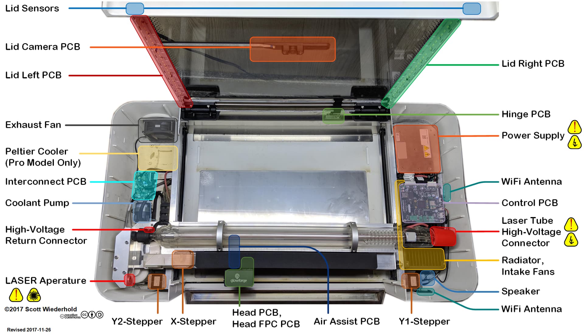
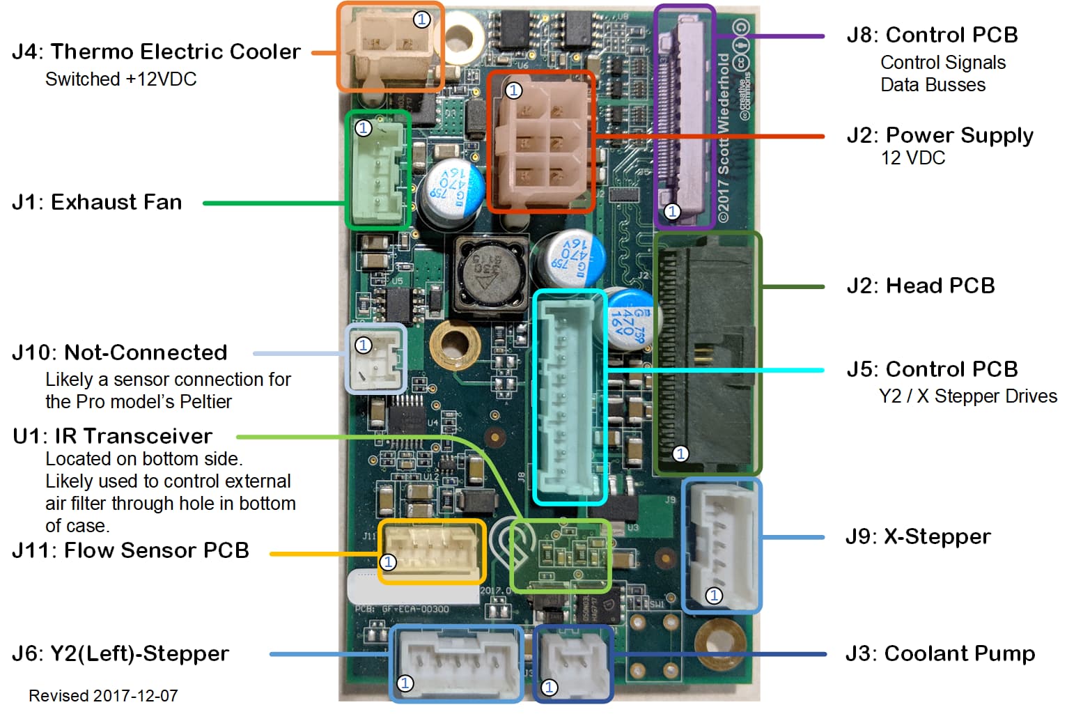
COMPONENT LOCATION:
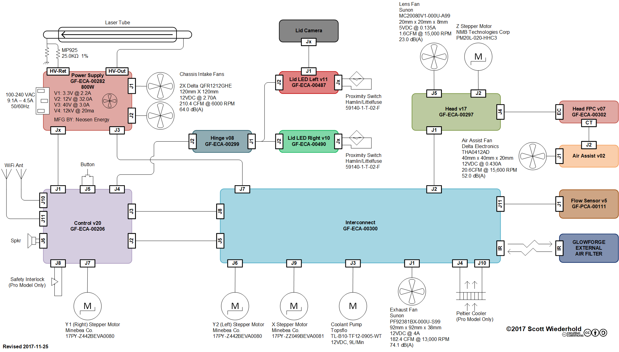
INTERCONNECTION OVERVIEW:
HEAD PCB:
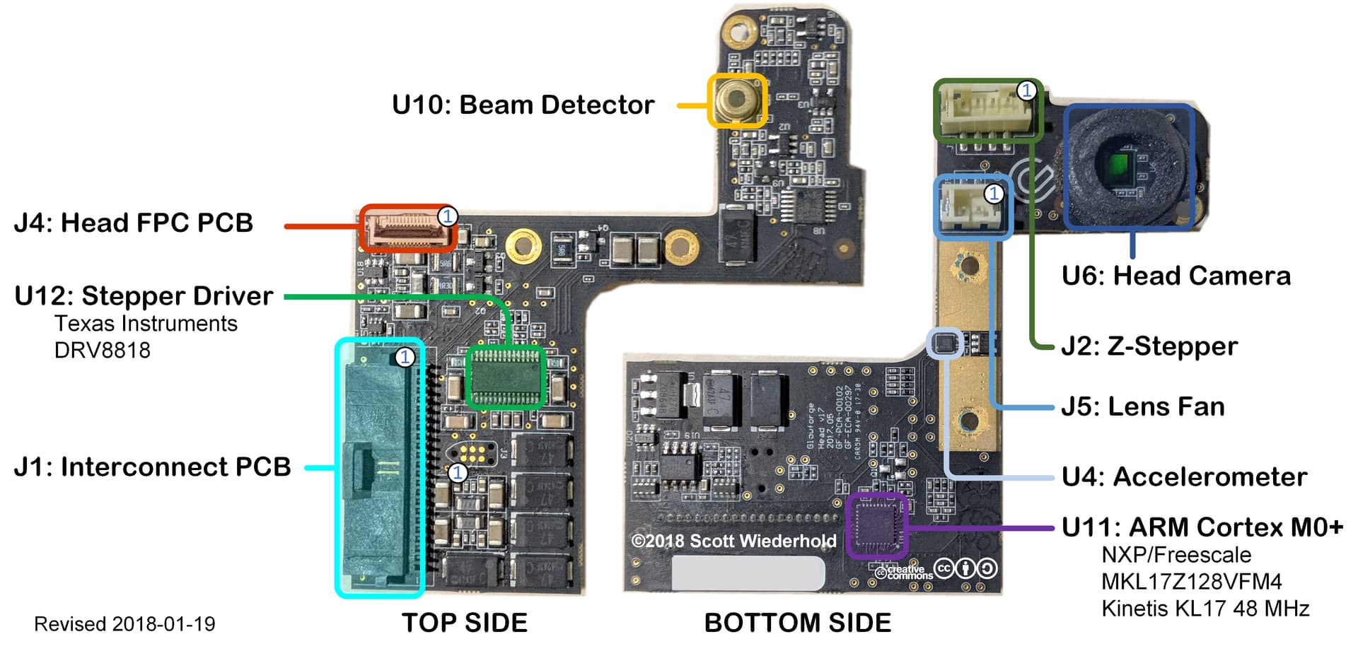
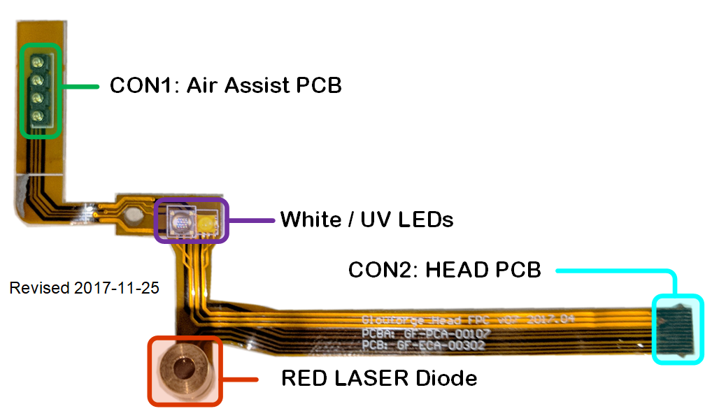
HEAD FPCB:
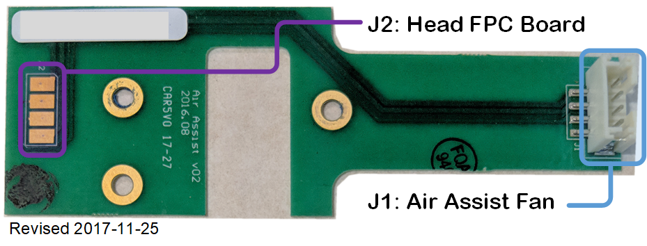
AIR ASSIST PCB:
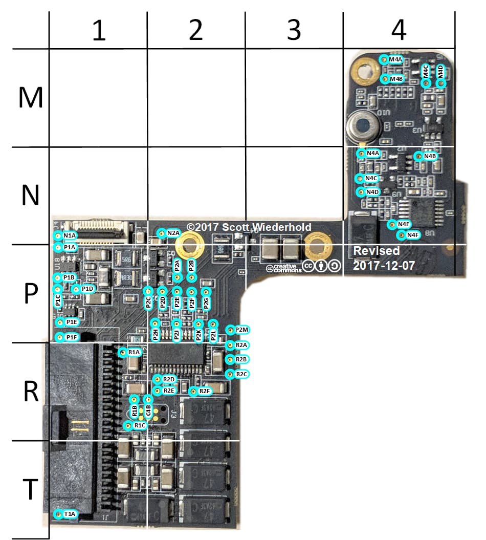
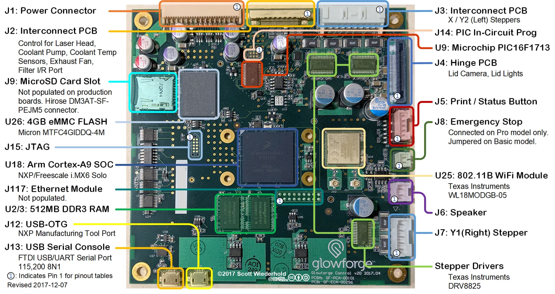
CONTROL PCB:
INTERCONNECT PCB:
It’s been 7 years, so there are likely revisions to these boards in newer models.
For one, they no longer populate the components for the USB serial port.
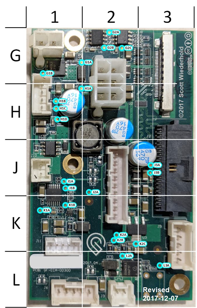
Most recent test point details (use at your own risk, as I make no guarantee of the accuracy of any of this):
| LOC | DESCRIPTION |
|---|---|
| +12VDC | +12VDC Power Supply |
| +3.3VDC | +3.3VDC Power Supply |
| +40VDC | +40VDC Power Supply |
| A2A | 40_VDC_ENABLE (J1_24)(U18_W24_GPIO5_IO17) |
| A2B | HV_ENABLE (Pulsed) (U24_2)(J1_16) |
| A2C | HV_PFC_STOP (J1_14) |
| A2D | LASER ON (J1_12) |
| A2E | INTAKE FAN 1 TACH (J1_10)(U18_P25_GPIO4_IO20) |
| A2F | HV_VOLTAGE (Connected to GND in pwr sply) U9_18_AN19 (J1_02) |
| A3A | HEADCAM_CSI_DATA0_N(U19_18)(J2_27) |
| A3B | HEADCAM_CSI_DATA0_P(U19_19)(J2_26) |
| A3C | HEADCAM_CSI_DATA1_N(U19_21)(J2_30) |
| A3D | HEADCAM_CSI_DATA1_P(U19_20)(J2_29) |
| A3E | HEADCAM_CSI_CLK_N(U19_23)(J2_24) |
| A3F | HEADCAM_CSI_CLK_P(U19_22)(J2_23) |
| A3G | Z_STEP (J2_19)(U18_G24_GPIO2_IO21) |
| A3H | Z_DIR (J2_18)(U18_H23_GPIO2_IO17) |
| A3J | HEAD (J2_16)(U18_E23_GPIO3_IO22) |
| A3K | BEAM_DETECT (J2_15)(U18_F23_GPIO2_IO31) |
| A3L | SERIAL_TX (U18_D19_UART2_TX)(J2_13) |
| A3M | SERIAL_RX (U18_E18_UART2_RX)(J2_14) |
| A4A | EXHAUST_FAN_PWM (J2_09)(U18_F17_PMW4_OUT) TP_A4A |
| A4B | WATER_FLOW_A (U9_5_ADC3)(J2_04) |
| A4C | THERM_ELEC_COOLER_EN (J2_01)(U18_B16_GPIO6_IO10) |
| A4D | EXHAUST_FAN_TACH (J2_08)(U18_D18_GPIO2_IO08) |
| A4E | WATER_FLOW_B (U9_4_ADC2)(J2_03) |
| A4F | WATER_PUMP_EN (J2_02)(U18_A16_GPIO6_IO08) |
| A4G | THERM ELEC TEMP (U9_7_ADC4)(J2_06) |
| A5A | Y_STEP_CURRENT (U9_22_RB1) |
| A6A | LIDCAM_CSI_DATA0_N(U19_12)(J4_27) |
| A6B | LIDCAM_CSI_DATA0_P(U19_13)(J4_26) |
| A6C | LIDCAM_CSI_CLK_N(U19_16)(J4_24) |
| A6D | LIDCAM_CSI_CLK_P(U19_17)(J4_23) |
| A6E | LIDCAM_CSI_DATA1_N(U19_14)(J4_30) |
| A6F | LIDCAM_CSI_DATA1_P(U19_15)(J4_29) |
| B2A | 12_VDC_ENABLE (J1_17)(U18_U25_GPIO5_IO08) |
| B2B | PWR TEMP (U9_2_ADC0)(J1_15) |
| B2C | LASER-HV PWM (J1_13)(U18_T25_PWM2_OUT) |
| B2D | INTAKE FAN 2 TACH (J1_11)(U18_P23_GPIO4_IO23) |
| B2E | INTAKE FANS PWM (J1_09)(U18_R22_PWM1_OUT) |
| B2F | HV_CURRENT U9_17_AN18 (J1_01) |
| B2G | MMC1 DATA 1 |
| B2H | MMC1 DATA 0 |
| B2I | MMC1 CLK |
| B3A | I2C_BUS4_SCL (U40_P7) |
| B3B | |
| B4A | |
| B4B | X_STEPPER_CURRENT (U9_3_RA1) |
| B4C | I2C_BUS4_SCL (J2_20)(U40_5) 12V |
| B4D | I2C_BUS4_SDA (J2_21)(U40_3) 12V |
| B4E | CAMERA_MUX_OE (U19_8)(U18_C15_GPIO6_IO07) |
| B4F | OV5648_MIPI_SEL U19_11 |
| B4G | X_FAULT (U18_E24_GPIO3_IO26)(U20_18) |
| B4H | I2C_BUS4_SDA (U40_P1) 3.3V |
| B4J | |
| B5A | X_HOME (U18_K25_GPIO3_IO06)(U20_27) |
| B5B | Y1_FAULT (U18_L24_GPIO3_IO08)(U21_18) |
| B6A | Y1_HOME (U18_M22_GPIO3_IO10)(U21_27) |
| B6B` | LID_LED_PWM (U9_21_PWM4)(J4_5) |
| C1A | 3.3VDC |
| C1B | U6_1 |
| C1C | U6_13 |
| C1D | U6_8 |
| C1E | U6_3 |
| C2A | MMC1_DATA3 (U18_B22) |
| C2B | MMC1_CMD (U18_F19) |
| C2C | MMC1_DATA2 (U18_A23) |
| C2D | MMC1_CARD_DETECT (U18_GPIO01_IO04) |
| C2E | USB_H1_DP (U18_E10) |
| C2F | USB_H1_DN (U18_F10) |
| C2G | USB_OTG_VBUS (U18_E9) |
| C2H | Voltage divider off of 3.3V rail. |
| C2J | GROUND |
| C2K | USB_H1_VBUS (U18_D10) |
| C2L | USB_OTG_DP (U18_A6) |
| C2M | USB_OTG_DN (U18_B6) |
| C2N | |
| C2P | |
| C3A | |
| C3B | |
| C3C | SUPERVISORY_RESET (U8_1) |
| C3D | NVCC_PLL (U18_E8) |
| C4A | |
| C4B | BOOT_MODE0 (U18_C12) |
| C4C | BOOT_MODE1 (U18_F12) |
| C4D | (U18_N7_NVCC_CSI) |
| C5A | 3.3VDC |
| C5B | IR SENS (U9_26_ADC13)(J4_P15) |
| C5C | IR SENS (U9_25_ADC11)(J4_P14) |
| C5D | IR SENS (U9_24_ADC9)(J4_P11) |
| C5E | IR SENS (U9_23_ADC8)(J4_P10) |
| C5F | |
| C6A | I2C_BUS1_SDA(J4_20)(U18_G23_I2C1_SDA) 3.3V |
| C6B | I2C_BUS1_SCL(J4_21)(U18_H20_I2C1_SCL) 3.3V |
| D1A | INTERLOCK_RESET (U23_6)(U18_P5_GPIO4_IO05) |
| D1B | BUTTON (U5_11)(U18_U6_GPIO4_IO09) |
| D1C | DOOR_SW1 (U5_1)(U18_T6_GPIO4_IO14) |
| D1D | LATCH_RESET (U18_R3_GPIO1_IO07)(U32_2) |
| D1E | U17_12 |
| D1F | LASER_ENABLE (U18_E22_GPIO2_IO30)(U17_10) |
| D1G | DOOR_SW2 (U5_3)(U18_T3{GPIO1_IO06) |
| D1H | U1_2 |
| D2A | |
| D2B | |
| D2C | |
| D2D | |
| D2E | (U18_U5_I2C2_SCL) |
| D2F | (U18_W4_HDMI_TX_CEC_LINE) |
| D2G | |
| D3A | |
| D3B | SERIAL_CONSOLE_TX (U18_M1_UART1_TX)(U37_15) |
| D3C | |
| D3D | SERIAL_CONSOLE_RX (U18_M3_UART1_RX)(U37_2) |
| D3E | |
| D3F | ??? (U18_R1_GPIO7_IO12) |
| D3G | (U18_T7_I2C2_SDA) |
| D3H | |
| D4A | C4D - Prefilter |
| D4B | |
| D4C | |
| D4D | |
| D5A | |
| D5B | |
| D5C | AUDIO_PWM (U18_B19_PWM3_OUT) |
| D6A | |
| D6B | SPEAKER_P (J6_2) |
| D6C | SPEAKER_N (J6_1) |
| E3A | |
| E3B | |
| E4A | |
| E4B | |
| E5A | Y2_FAULT (U18_N23_GPIO3_IO14)(U22_18) |
| E6A | AUDIO_ENABLE (U18_F25_GPIO5_IO04) |
| F3A | (U13_5) |
| F3B | |
| F5A | Y2_HOME (U18_M21_GPIO3_IO09)(U22_27) |
| F5B | |
| J1A | THERM_ELEC_COOLER_TEMP (U4_8_OUT3)(J5_26) |
| J3A | I2C_BUS4_SCL (J2_10) |
| J3B | I2C_BUS4_SDA (J2_9) |
| K1A | WATER_FLOW_A (U4_1_OUT1)(J5_28) |
| K1B | WATER_FLOW_B (U4_7_OUT2)(J5_29) |
| M4A | |
| M4B | |
| M4C | |
| M4D | |
| N1A | Air Assist PWM (J4_6) |
| N2A | |
| N4A | |
| N4B | |
| N4C | |
| N4D | |
| N4E | |
| N4F | |
| P1A | (J4_10) |
| P1B | (J4_12) |
| P1C | Air Assist Tach (J4_7) |
| P1D | (J4_11) |
| P1E | (U11_16_PTC5)(U1_5) |
| P1F | (U11_22_PTC1) |
| P2A | |
| P2B | |
| P2C | J4_01 |
| P2D | J4_03 |
| P2E | I2C_BUS4_SDA (U11_21_PTB1) |
| P2F | I2C_BUS4_SCL (U11_20_PTB0) |
| P2G | |
| P2H | Z_MODE0 (U12_P13)(U11_17_PTA18) |
| P2J | Z_STEPPER_CURRENT (U12_8_VREF) |
| P2K | Z_DIR (U12_3_DIR) |
| P2L | Z_HOME (U11_18_PTA19)(U12_1_HOME) |
| P2M | |
| R1A | (U11_14_PTA4) |
| R1B | |
| R1C | |
| R2A | (U12_10_VCC) |
| R2B | |
| R2C | 12VDC |
| R2D | (U12_17_RESETn) |
| R2E | Z_STEP (U12_19_STEP) |
| R2F | Z_ENABLE (U12_6_ENn ) |
| R2G | |
| T1A |
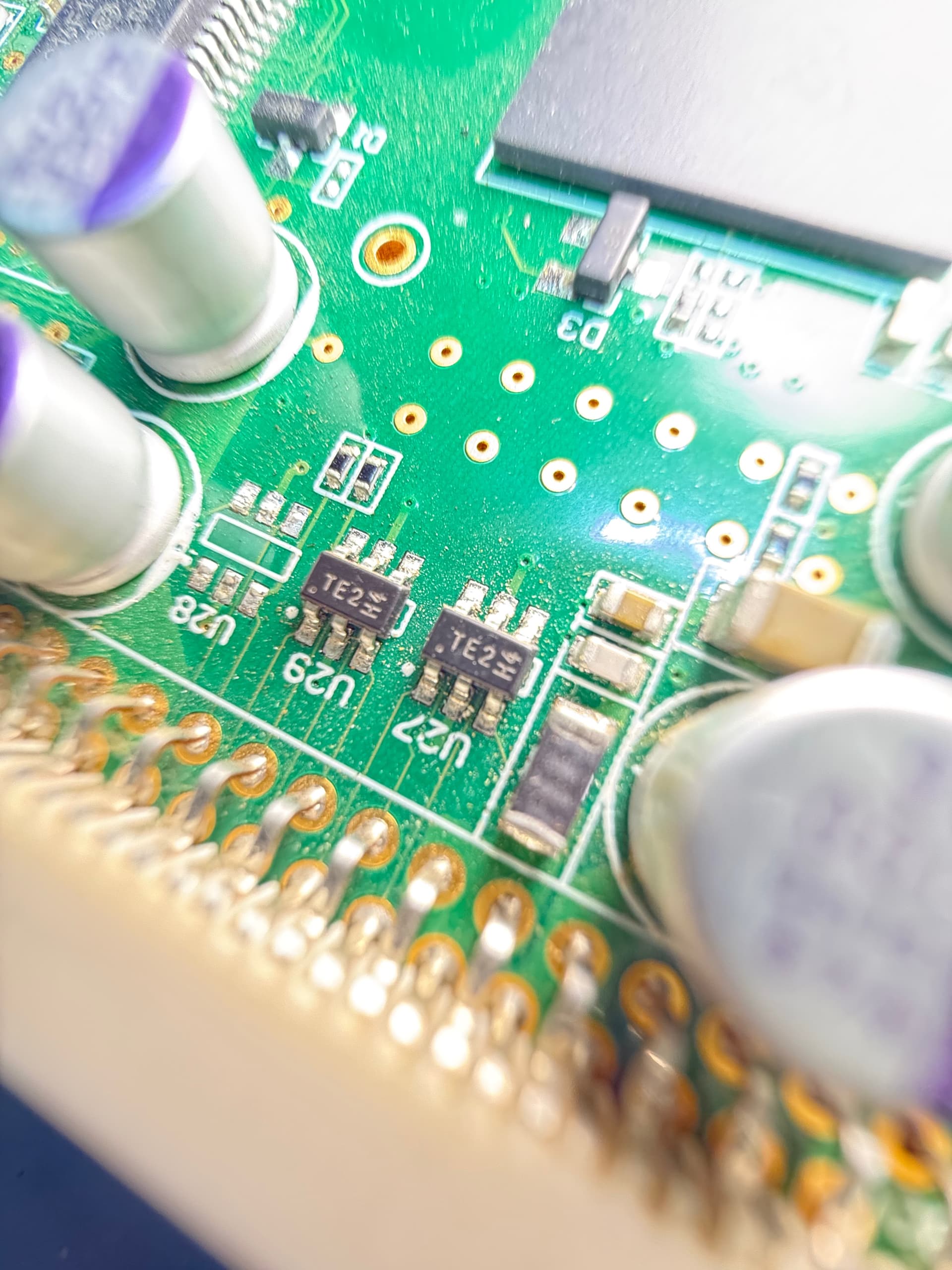
Hi @ScottW514 any chance you can help me identity this component? U28 on the main board, same as U29 and U27 which have the marking “TE2 H4”?
It had a short on a board I had and I fixed it by snagging on from another board. But the other board was working so I’d love to get a replacement for that board.
Also, what is the connector model number of J4?
Thank you!
1 Like
U27,U28, and U29 are rail-to-rail ESD protection devices.
A handy reference for this type of adventure is the OpenGlow schematic. It was designed as a drop-in replacement that is connector-for-connector/pin-for-pin compatible with the OEM control board.
From the OpenGlow schematic (NOTE: I used a slightly different ESD/EMI protection scheme):
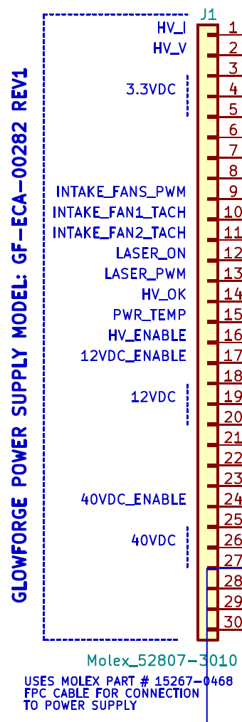
There you can see the pin assignments for the power supply connector (J1).
U28 has the following connections:
| PIN | Connection | Description |
|---|---|---|
| U28-1 | J1-1 | HV Current Feedback |
| U28-2 | GND | |
| U28-3 | J1-10 | Intake Fan #1 Tachometer |
| U28-4 | J1-9 | Intake Fans PWM Out |
| U28-5 | 3.3VDC | |
| U28-6 | J1-2 | HV Voltage Feedback |
As this is strictly a passive protective component, and assuming there are no other problems in the system, the donor board will still operate fine without that part. However, as you have experienced, ESD spikes do occur, and those devices do a great job of protecting the signal lines (often at their own expense) - preventing damage to devices that are much harder to replace (like the microprocessor).
A suitable replacement would be something along the lines of this:
As to J4, you can also find the part number for that on the OpenGlow schematic:
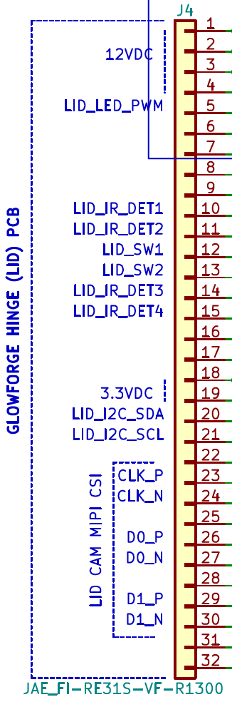
It is made by Japan Aviation Electronics, part number F1-RE31S-VF-R1300.
Thank you! Do you know the spec of the mating connector to the F1-RE31S-HF-1500 that they used? I want to make a replacement cable but can’t seem to find the connector they used anywhere (Axon)…
There are a number of types available, and they are listed at the bottom of the page that I linked to (look for the “Combination” row).
JF08R0R041020UA is the closest to the OEM, as it uses a FPC (flexible printed cable).
The problem is that Glowforge uses bespoke cables. These are custom printed cables, with 3rd party connectors manufactured as an assembly by Axon Cable.
I do not know of anyone who has successfully made one. In theory, you could design and order the FPC from one of the many PC board manufacturers, and then attach the plugs.
Edited to add:
These may work (use 600mm and 900m lengths):
Unfortunately those are 41 pins and not 31.
The hyperlink for F1-RE31S-VF-R1300 goes to FI-RE41S-VF-R1300, which is 41 pin. The correct link should be https://www.jae.com/en/connectors/series/detail/product/id=65252&type_code=T1040, for which there isn’t the same type of connector unfortunately.
Good catch. I updated my link.
Hi @ScottW514 Which one of these TVS diodes would you recommend
Thank you!!
Exact replacement is Diodes Incorporated D1213A-04TS
https://www.digikey.com/en/products/detail/diodes-incorporated/D1213A-04TS-7/3340451
I tested my control board while running and I don’t have 40v A2D is also low. Power supply?