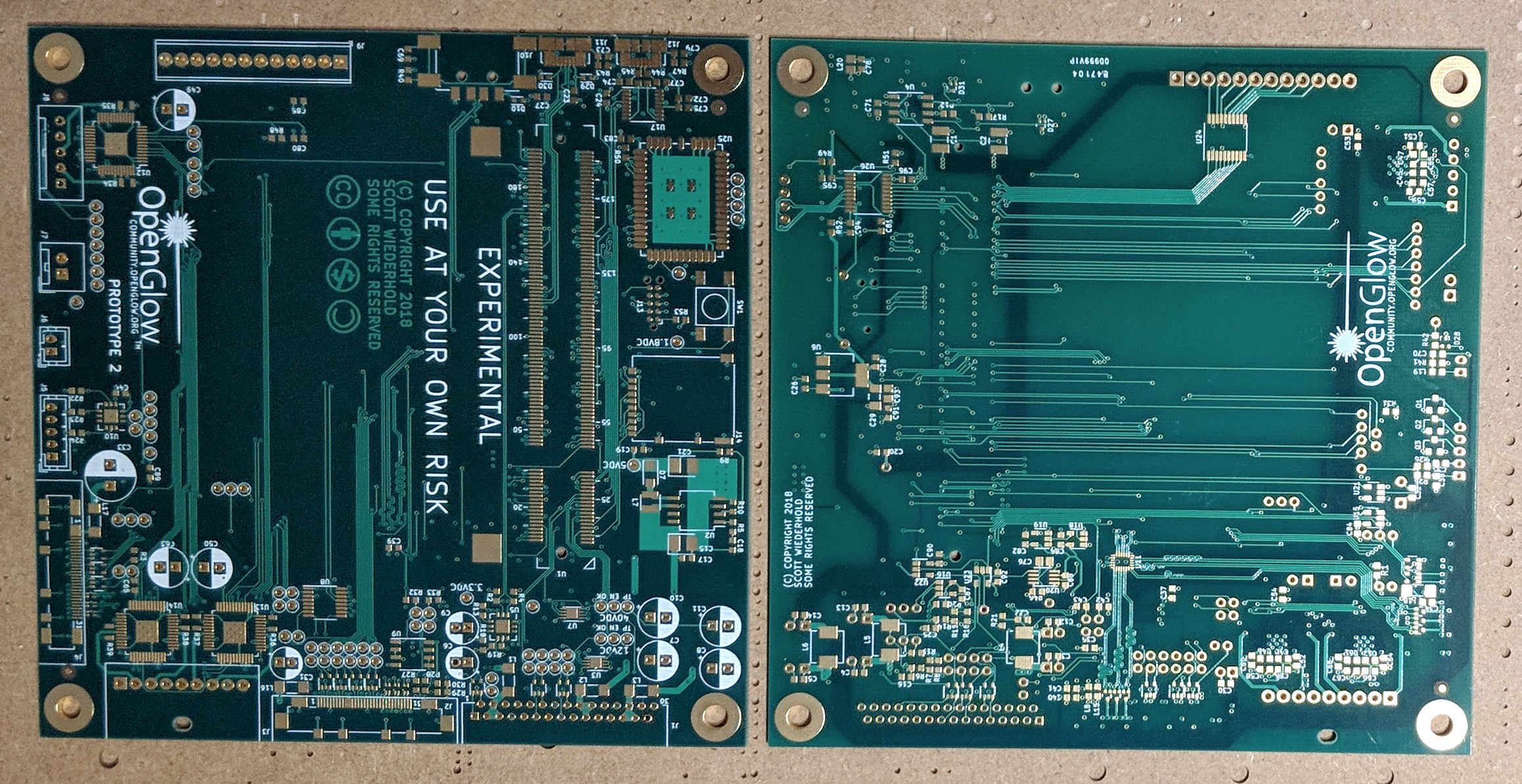
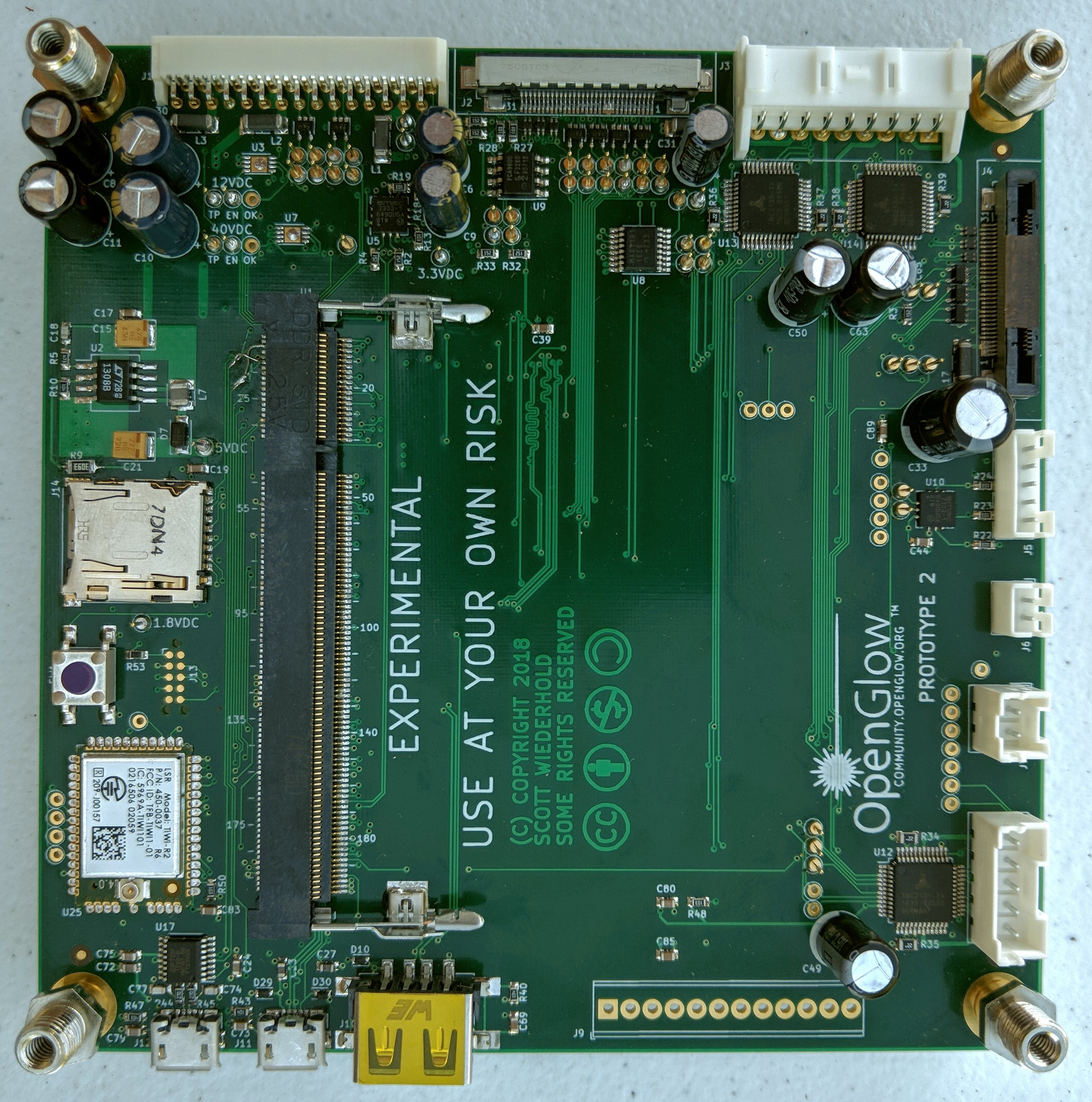
The PCB’s for Prototype #2 arrived yesterday from Seeed.
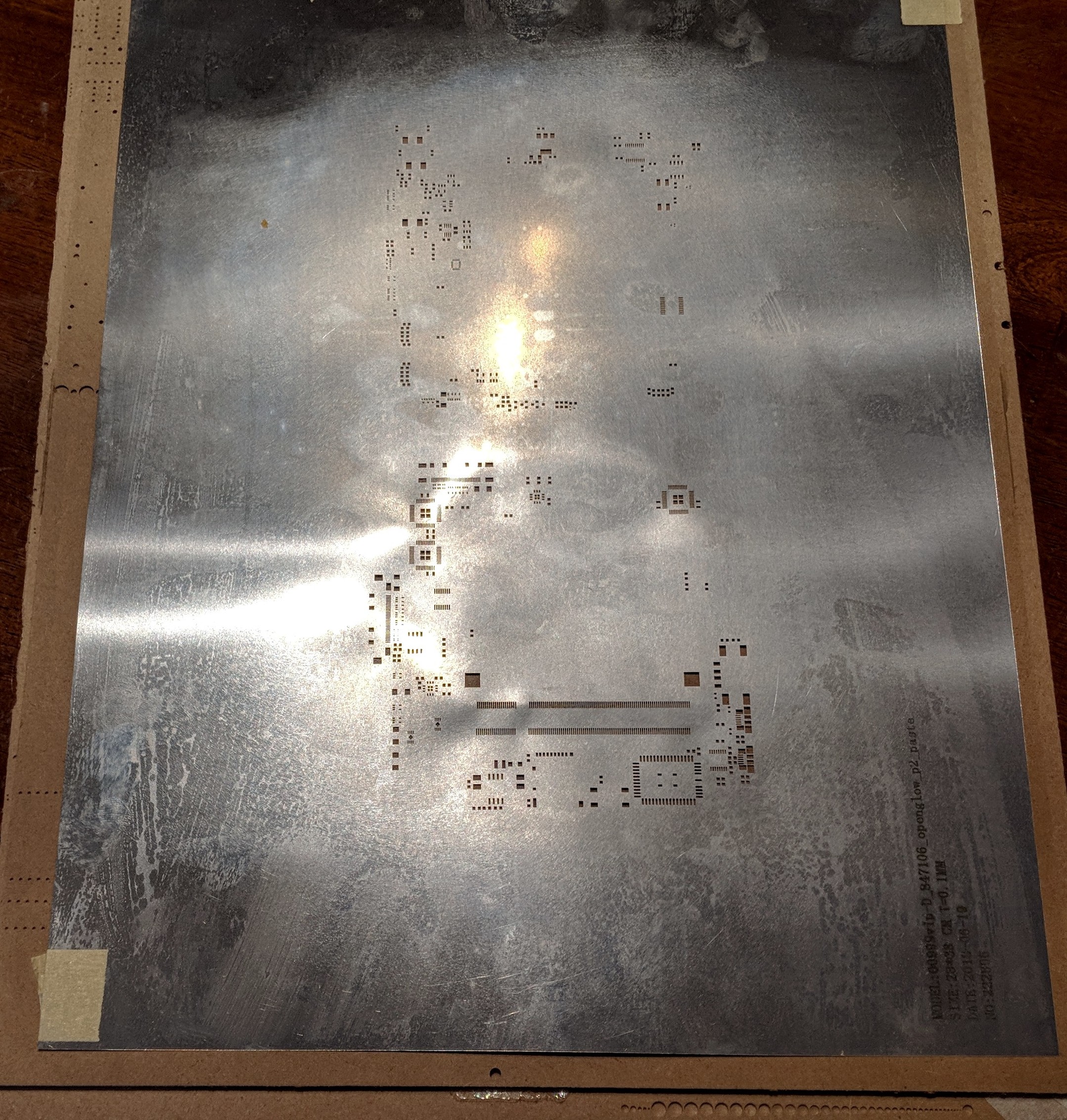
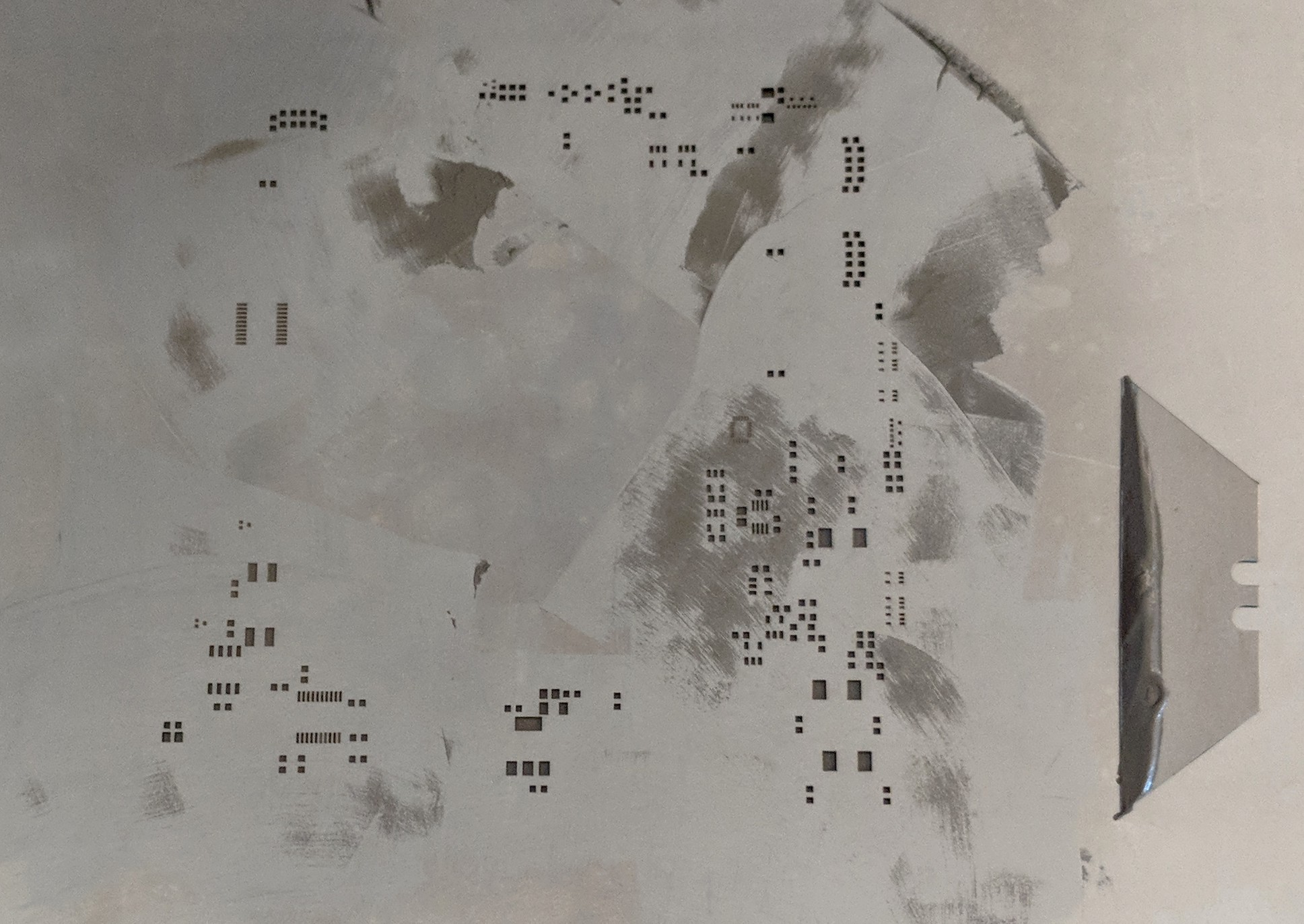
Quality on the PCB’s is about the same as the last prototype. The stencil, on the other hand, sucked. It has significant warps - mostly in the top side area. It is very difficult to photograph the warps, but you can get the idea by looking at the waves in the reflections. At their worst, they lift almost 2mm above the base plane.
I gave it a go for the bottom side, and it worked out OK.
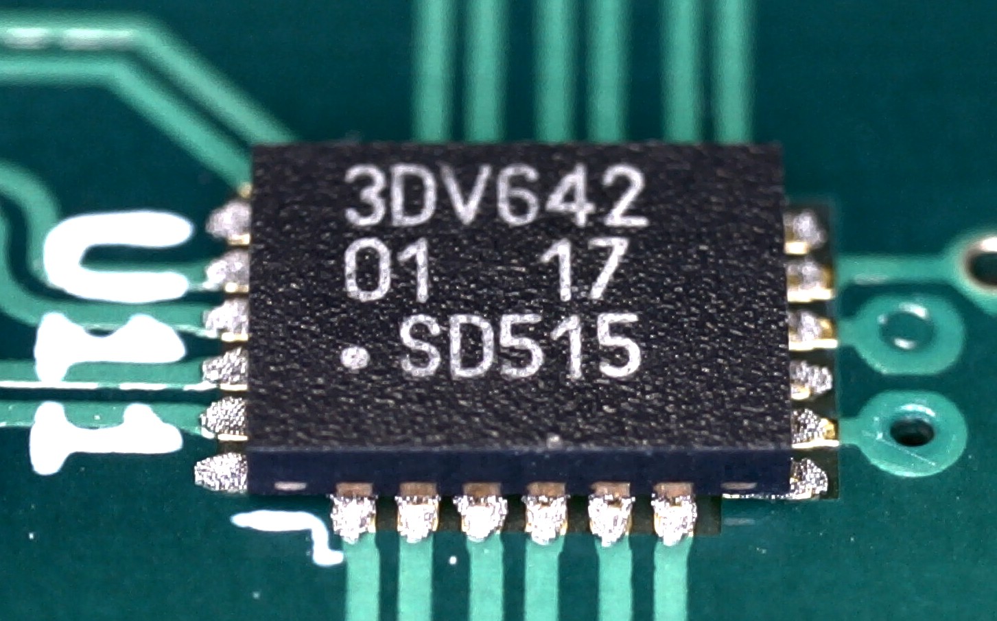
The most crucial registration is on the NX3DV642 MIPI switch for the cameras. That little sucker is only 2.5mm x 3.4mm with a 0.4mm pin pitch. As you can see, the stencil worked pretty well (and my hands were pretty steady, too!):
Bottom side is fired, and looking good. I’m going to tackle the top side tomorrow.
5 Likes
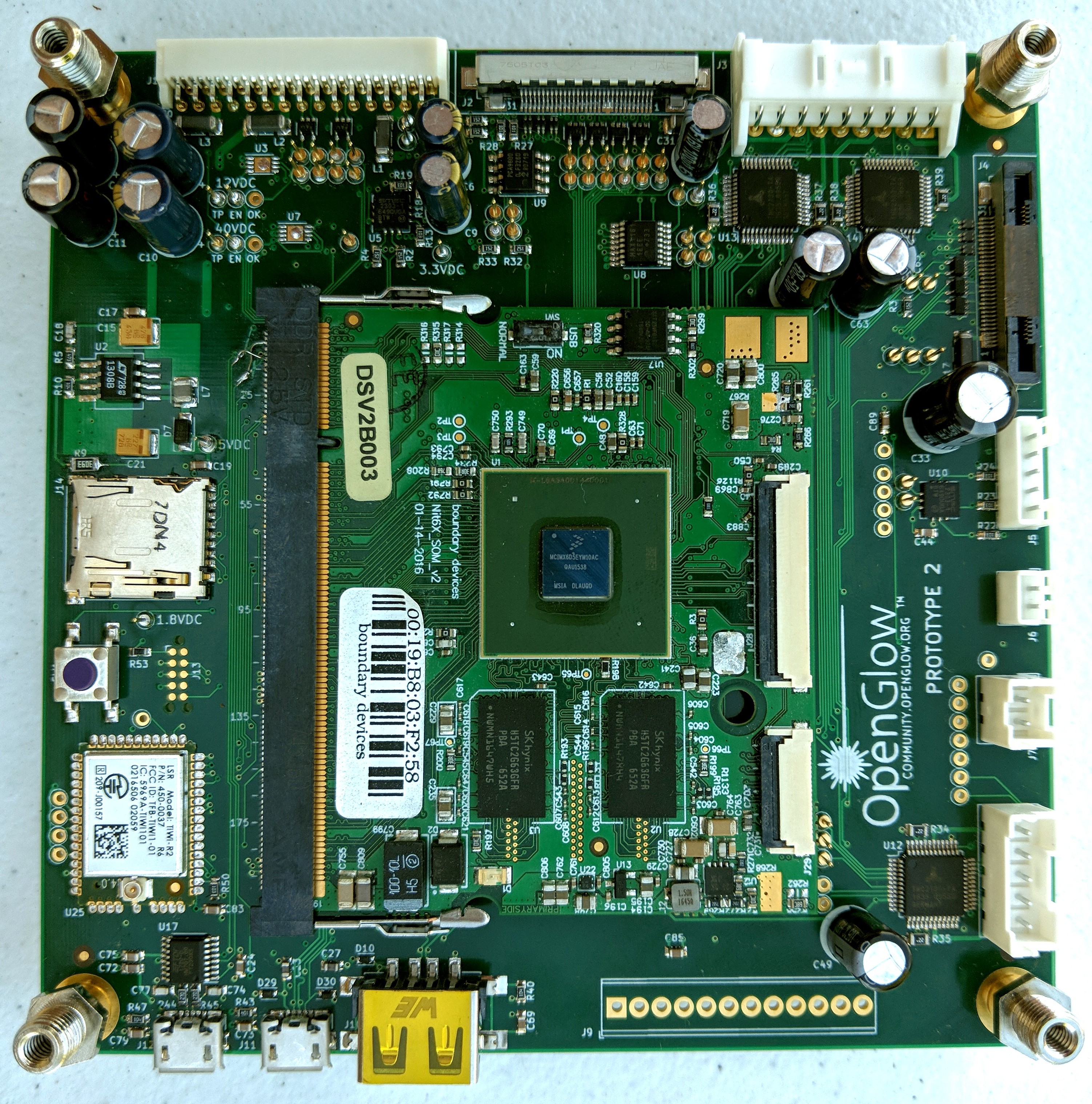
Board fully populated:
The stencil made a few areas a nightmare. I’ll spare you the details…
I also found a few problems with KiCad footprints that I missed. Ugh.
So far, I’m pretty happy with where it’s at.
3 Likes
Throwing out a quick status update:
The new board is up and running.
I already have a couple goofs that will necessitate another board revision. Nothing that hasn’t easily been worked around, so far… C’est la vie.
All communication buses are live and talking with both on-board and Glowforge peripherals.
Wireless, USB, and Serial interfaces are also functional.
I am in the process of making the needed code changes to support the new IO assignments and writing the modules for the new hardware. This will be the most time consuming part. You can watch my repo commits for details on that progress (which reminds me, I have a few to push).
I’m going to setup a Wiki category here, and start the documentation process - system by system. I need to get my chicken scratch notes formalized and shared.
4 Likes